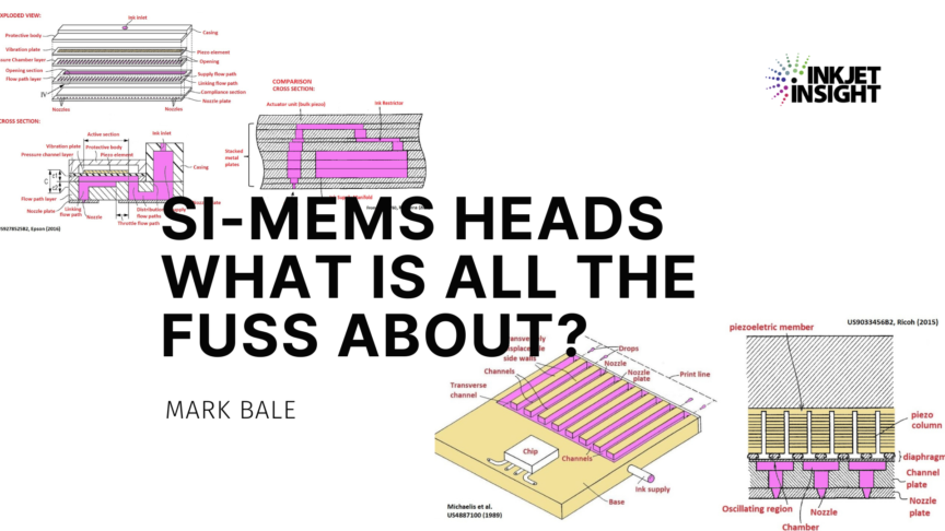
We all love our acronyms, right? Well, in print head terms the one that gets a lot of coverage is “MEMS”. In our webinars about print heads, last year we looked at different print tech and what it means for different inkjet printing systems and processes. In this article we explain a little more about why we hear so much about this buzz-phrase with reference to latest print head technology and try and explain a little print head manufacturing jargon along the way.
Just do a web search with your favorite engine, you’ll probably end up with a wiki page near the top hit. It will no doubt explain the acronym as Micro Electro-Mechanical Systems. Taken literally it means “small things that can move in response to electrical signals”, or conversely something that can respond to motion and produce an output. That encompasses an incredibly wide range of potential industrial applications and lifestyle devices in our modern world, from ultrasound imaging for medical diagnostics to smartwatches for fitness and health tracking and microphones and even the microphones for your cell phone.
Deep Dive into MEMS has Meaning
As the print world, as well as almost every other industry is moving to using such technology in one form or another, it is valuable to understand what you are working with. Integrating print heads into any part of your printing or manufacturing process should not be a daunting task. We have been moving deeper into the inkjet print heads in a detailed fashion through technical blogs and webinars. This article will dive deeper into the intricacies of the inkjet head structure and address the differences which affect life span and performance of the printhead.
Slicing and Dicing
The literal definition of MEMS happens to describe almost any (piezo) inkjet print head from a mainstream supplier for the last 20 years since most ink channels are <<1mm, and therefore “micro”. As an example, one of the key steps for making heads from the like of Xaar, KM, Seiko and TTEC is to cut the ceramic PZT (piezo electronic) material with saw to make the parallel channels smaller than 1/10th of a millimeter. This dicing method is also used to separate the PZT stacks in Ricoh heads and is directly borrowed from the techniques developed for making ultrasound imaging devices.
Si-MEMS Manufacturing
For print heads the term is usually being used to describe the methods of manufacture with silicon – that same element that has transformed our lives through the 20th century when used for making computer chips. That’s why we’ve refined the terminology to Si-MEMS (short for “silicon-MEMS”). The big print head manufacturers have been steadily taking advantage of the manufacturing methods that have grown around more common MEMS uses, like sensors for airbags. Their aim is to to industrialize the production of heads to be both scale-able and reproducible at a very fine scale. The first print head folks to apply Si-MEMS techniques were those making thermal print heads for consumer markets, like HP and Canon even though TIJ and bubblejet heads are not literally MEMS, since they don’t have moving parts!
I was lucky enough to spend some of my formative years during my PhD figuring out how to make small things out of both silicon and PZT (lead zirconate titanate), the important component in many piezo print heads. Therefore, I have a real passion for learning how print heads are made and figuring out how that can influence what they can do. In the next few blogs, I hope to share some of that nerdy knowledge & discuss some of the basics, using plenty of pictures to try and explain what differentiates this amazing technology.
Etching and Precision – Some Background
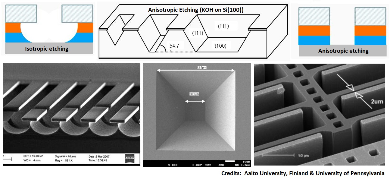
When you try and make something measured a few tens of microns (millionths of a millimeter, um), like an inkjet nozzle, the best way is to use photolithography. A long word perhaps, but a nicely literal word for a method of masking and etching materials using a polymer material patterned by light. It is a bit like a special UV ink coating that can be developed like an old photo film & then selectively withstand the high and low pH chemistry used to etch metals, and of course silicon. The issue with wet etching an amorphous or polycrystalline material (like a metal) is that it etches all direction equally. However, if you have a single crystal of silicon, you can etch preferable in one direction using something like potassium hydroxide (KOH), which allows some unique shapes to be made.
Wet etching is messy though, so the silicon chip folks came up with the idea of using a plasma to do the job. This means loading your sample into a vacuum and introducing a specific nasty gaseous element, and then getting the gas all excited using electricity. To put that in a print context: the bright sparks of a corona treater is a type of plasma in air. With a bit of clever development, the engineers got the plasma to work preferentially in one direction and thus deep etching was possible. You might hear the phrase used by some manufacturers DRIE, usually said as dee-are-eye-ee, although it is also a bit of a pun on the fact that plasma etching is often called “dry” etching.
So What?
So why risk putting you off your coffee with all this microfabrication stuff? Well, it helps explain the things that really matter for those wanting to know what makes Si-MEMS better. It all comes down to that precision. Compared to the cutting/drilling/sticking approaches still used in manufacturing of many leading print heads, the parts made of silicon have an incredible level of repeatable dimension. Dimatix caught onto this early when the glued a silicon faceplate to their popular S-class head to create new “SQ” product to meet the needs of drop placement accuracy. Back in the early 2000s I used it to make OLED devices. This then led to their Sapphire Q-class heads, which are still a stalwart of the inkjet industry in some pretty well-known graphics printers.
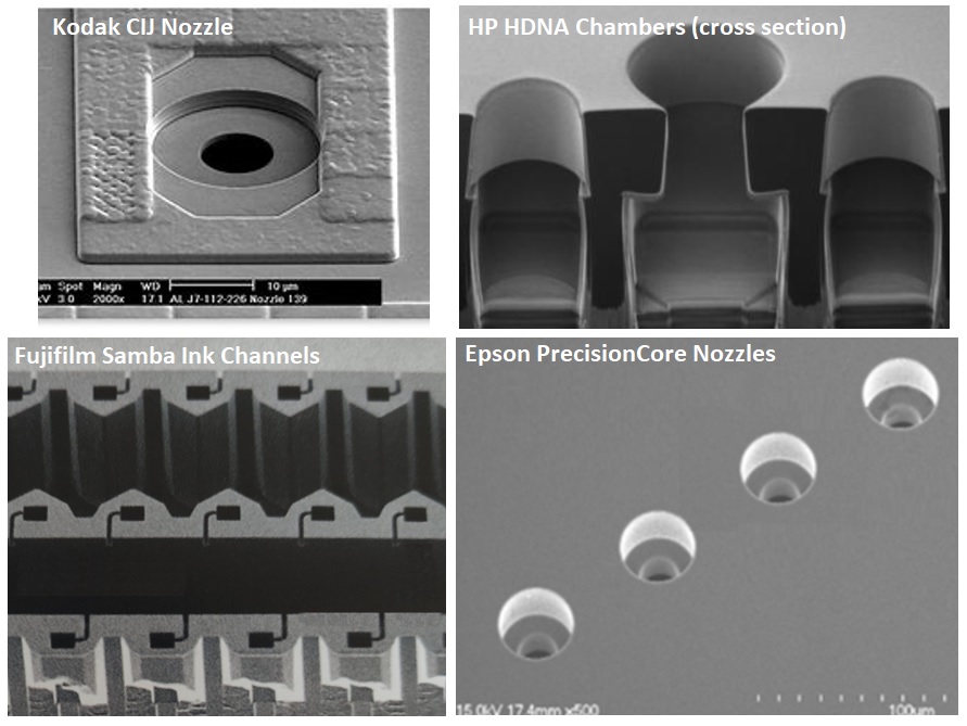
That precision can be scaled to create arrays of nozzles that are limited only by the ability to somehow supply the ink. At 1600 nozzles/inch, the Memjet head is good example of just how dense the nozzle arrays can be made, since the “footprint” of the heater is much less than the space need for a piezo actuator. In comparison, the highest resolution in a single nozzle row is achieved by Epson in their Precision Core™ heads, at 300dpi. By creating arrays of nozzles then higher overall resolution such as 1200dpi can be achieved. The Fuji Samba is a great example and has 32 rows of nozzles in a single chip. See the image below for some examples, including the Kodak Stream CIJ technology which uses a heater around the etched silicon nozzle.
Being an automated batch fabrication technology, the other thing Si-MEMS enables is the potential for lower cost. This has been demonstrated most notably with thermal heads, where the head is treated as much more of a consumable due to the lower cost per unit. Although it is is helped by the slightly simpler structure of thermal heads, Effective cost reduction with Si-MEMS is only possible with the economies of scale, which is why it made sense for Fujifilm to sell their breakthrough Si-MEMS head Samba outside of the sheet fed Jetpress inkjet print technology in which it was originally launched.
The downsides for those developing the heads, rather than those using them, is that all silicon processes are based on wafers, where defectivity in production can easily cause failure. It is important to optimize the process to achieve a high yield, as well as to achieve the right design/geometry in order to avoid scrapping a lot of your precious chips. Since the processes are complex and take time to iterate the whole operations is an expensive commitment, and thus remains the purview of only the biggest inkjet companies. This is a contributing factor to why independent UK manufacturer Xaar’s withdrawal of their promising XJ5601 head.
A Quick Mention of “Thin Film”
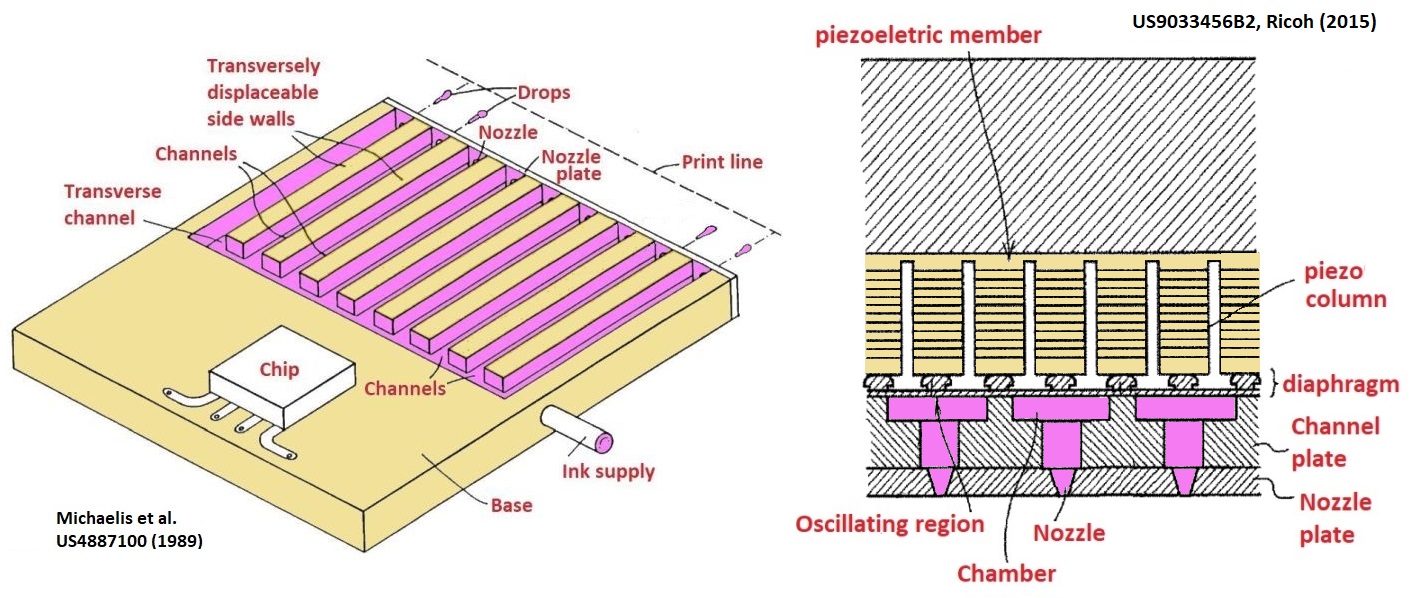
When making heads with Si-MEMS technology, then the complex channels delivering the fluid to the important parts of the head are created by multiple silicon wafers with different additional grown/deposited layers of both metals and silicon compounds (like SiO2 and Si3N4) to make the necessary flexible and rigid structures. A crucial development is that the piezo itself is also deposited on the silicon, rather than being cut down from a bigger piece and glued on. This means the whole chip part can be made in the silicon factory (or Foundry). Since a deposited piezo layer tends to be tricky to make too thick, all recent Si-MEMS heads are known as thin film devices. This term, which is nice and literal, distinguishes the head design from the traditional piezo heads which have generally become known as “bulk” type (because the PZT starts life as big piece before being processed).
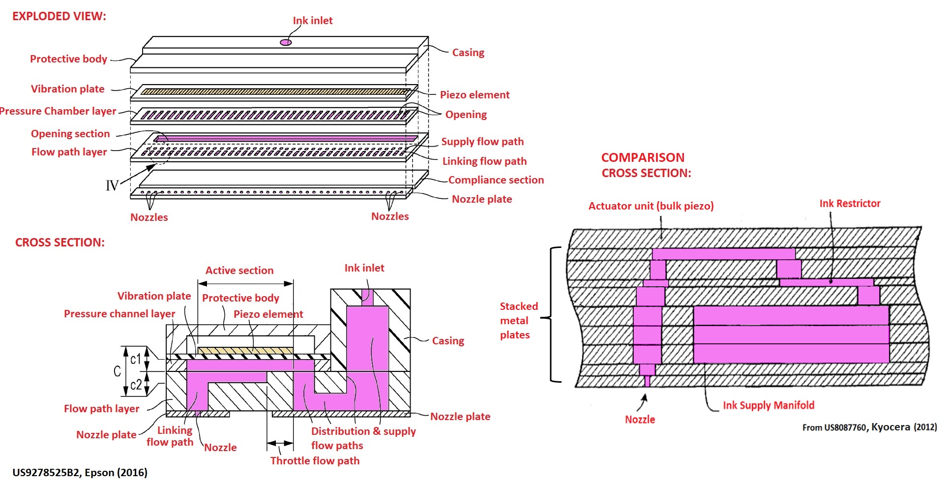
Compare the left-hand patent image below to those above and you can see that the thin film of piezo usually sits in the top layer above the nozzle and ink channels and is itself patterned. The “roof” actuator design is not unique to Si-MEMS heads since bulk heads also have them – as also shown using second edited image from a Kyocera patent for comparison. In that case, however, the actuator is a continuous bulk piece sitting on top the stacked of metal plates making up the ink path. Another difference between the two is the number of plates being used. Note how the use of silicon tends to reduce the number of layers needing to be aligned to typically 3-4, but that patterning each wafer from both sides can create more internal structure to control the internal ink flow. This accurate control of channel design is very useful for creating recirculating paths as can be seen in the Samba photo above.
Finally, if you are looking at different printhead suppliers you might hear some discussions about the way these thin films are made, and that some are better than others. The two biggest methods are solution processing (“sol-gel”, used by Ricoh, KM, Epson) and vacuum deposition (“sputtered”, used by Fujifilm). Both types of process have been demonstrated to result in actuators that achieve a very large number of firing events before performance reduces, so the important thing to know is that they all are likely to last longer than the typical head install time, especially if the printing system does not manage the ink properly and avoid it drying in the head.
We hope that gives an Insight into what is meant by “MEMS” but do let us know if you have any questions or comments about the content. In our next tech blog we’ll be getting back to discussing a bit of chemistry.