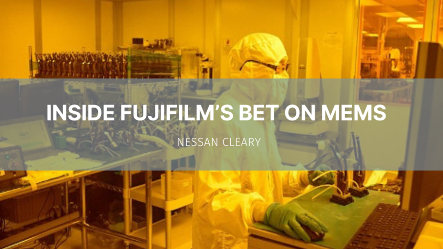
Over the last couple of years Fujifilm has been quietly upgrading the Dimatix manufacturing plant in Santa Clara, California, which is home to the Samba printhead. So I went to have a look at the factory, to get a better understanding of how the MEMs manufacturing process works, and what this means for the resulting printheads.
Dimatix has two manufacturing facilities, both in the US. The company’s main base is in New Hampshire and is home to most of Fujifilm’s printhead portfolio, including the StarFire and Saphire series, all of which rely on bulk piezo technology. The Santa Clara plant, which is in the heart of America’s Silicon Valley, is a very different proposition. This was specifically set up to use the MicroElectrical Mechanical systems or MEMs approach. Essentially this means using semiconductor technology to construct the actuator, which allows for greater complexity and precision.
And, as Bailey Smith, EVP of business development, points out, that in turn meant establishing a base in Silicon Valley: “If you want to do MEMs there are only a couple of places you can do it. There is a ton of silicon MEMs facilities here and Silicon Valley. You have to have the nitrogen gas and the chemical storage expertise we have. Trying to recruit those people in New Hampshire would have been impossible.” (The plant consumes a great deal of liquid nitrogen, which is used to create an oxygen-free atmosphere within the production equipment in order to prevent the copper in the electronic circuits from oxidising.)
Dimatix, which was set-up in 1984, took the decision to invest in MEMs, when the company was still owned by Markem Corporation. To get the ball rolling, the company acquired some silicon fab equipment which at that time was already 10 years old.
At the same time, Fujifilm realised that digital would eventually replace offset printing and was looking to inkjet as a way to replace its CtP business. To that end, Fujifilm had already started development work on its JetPress inkjet press. That eventually led the company to acquire Sericol, which developed UV inks, in 2005 and Avecia, which specialised in aqueous ink, in 2006, followed by Dimatix, also in 2006. Smith notes: “Fujifilm at its core is a technology company. They want to own the technology for the products they are producing.”
He continues: “They knew that the JetPress needed high print quality and they had already started working on MEMs in Japan. But when they saw what we had been doing they were interested.”

Fujifilm Dimatix set up a dedicated facility in Santa Clara for MEMs manufacturing.
Dimatix’s initial efforts with MEMs were based around bulk piezo. But Fujifilm had already developed a different approach, sputtered PZT, which proved far more effective and was adopted by Dimatix. Smith explains: “Fujifilm in Japan have the core patents. They licensed us the technology and we adapted it to make it production worthy. And we have made customisations to the tools which was a lot of work.”
It should be pointed out that sputtered PZT is one of several methods that can be used for MEMs fabrication of printheads. It’s quite distinct from other methods, such as SolGel, which have been adopted by other printhead manufacturers. Smith says that sputtered PZT is more robust and leads to heads that are better suited for industrial production, but of course, other manufacturers will say the same about their heads!
Most of today’s piezo drop-on-demand printheads use lead zirconate titanate, usually referred to as PZT, because of its very efficient piezo-electric properties, where it changes shape when an electric charge is applied. Piezo printheads use this shape shifting to force the ink from the ink chamber through the nozzles.
Fujifilm’s approach is to use a form of RF-magnetron sputtering to create the thin PZT film layers on the silicon substrates, giving it a piezo-electric coefficient of d31 = -250pm/V which is said to be around 70 percent higher than conventional PZT film. This is largely down to using a high level of Nb dopant of around 13 percent as well as a very precise control over the way the crystals are aligned, which is essential in order to control the way that the PZT will distort.
Smith says that the major advantage of this approach over other techniques, including SolGel, is the poling of the PZT: “The sputtering process that we have created is unique. With bulk piezo they are putting in lumps and forming crystals that then have to be aligned with poling at very high temperatures and that’s quite a challenge. When we deposit our PZT it’s already aligned so there’s no high temperature processing which means there are things that we can do to the MEMs structure.”
He continues: “One of the measures we have is how much deflection we have from a given wavelength and we are one of the top for that in the world. And we can de-pole them if we apply too much temperature. We feel that we have the best PZT and lots of other companies come to us to use ours.”
He adds: “We have a small group of people that work in R&D at other potential applications for MEMs using sputtered PZT, which is world renowned for this type of work. We do some of the development here for the products that are going to be built in New Hampshire. It’s just for engineering and development, not production. We also work in the ultrasound space and some medical devices but that’s not our primary space.”
Larger wafers
Micro Electromechanical systems combine electronics with moving parts, allowing complex designs to be executed in very small spaces. There is a limited choice of materials for building these systems, with silicon being by far the most common because of its long service life and the ease of incorporating electronic functionality. Consequently Si-MEMs can be built using a similar process to making semiconductor devices. Thus the materials, such as silicon with a thin film of PZT, can be deposited one layer at a time, using photolithography to make the patterns within these layers to create the channels for electronic circuits and fluidic management.
Every Samba printhead has an EPROM module with information on its performance.
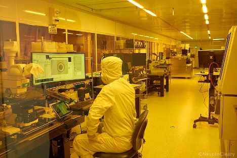
The process starts with photo lithography. Smith explains: “It’s a semi conductor process. So we go through multiple layers building up the processes. We have maybe 20 layers and each of the features is added in these various layers. So we add each feature one at a time. And then we stack it up and do the metallisation features.” These features include a separate layer for the fluidic management for recirculation.
This work is done with ASML steppers, supplied from the Netherlands. Smith notes: “ASML are the most advanced in the world next to TSMC of Taiwan which are just different geometries.”
Smith adds that Dimatix is using a more specialised variant: “This photo tool is because we have patterns on both sides of the layers so we have to align features on the front to features on the back. That leads to specialised handling. We can’t just run the wafer through on a tool because we would be scratching the bottom of the wafer so we have to protect both sides of the wafer but the ASML steppers are very reliable.”
Darren Imai, vice president of MEMs R&D for Fujifilm Dimatix, points out: “These are very delicate structures, ranging from about 400 to 650 microns and sometimes it can be down to 10 microns so that’s quite specialised work to handle that kind of geometry.”
Over the last couple of years Fujifilm has adapted some of the fab tools to create larger wafers, up from 6ins to 8ins. The dies that form the basis of the Samba printheads are cut directly from these wafers. So the immediate benefit of the larger wafer size is an increase in manufacturing capacity. The 6ins wafers can yield 10 dies, but this goes up to 21 dies with the 8ins wafers.
In addition to this extra capacity, the upgrade to the equipment has also yielded better results, as Imai explains: “We were able to get the uniformity of the PZT across the 8ins much more effectively than 6ins.” He says that changing to the larger wafers involved quite a lot of capital and a lot of hard work, noting: “We have improved the uniformity across the platform. As we have upgraded a lot of the equipment, some of which was 30 years old. We went to new more state of the art equipment which gives us more process advantages.”
One of the challenges in moving to the larger wafer size was the need to keep manufacturing at the plant whilst upgrading the machines, which also limited the size to 8ins. Fujifilm was able to upgrade its existing tools to handle the 8ins wafers but would have had to start from scratch for a larger size.
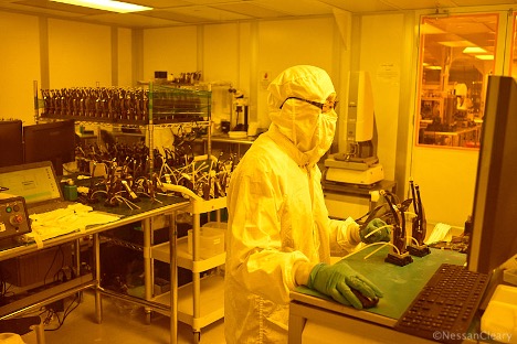
The dies form the basis of the Samba printhead, containing the electronics and the fluidic channels. However, this is not the whole story as a number of other components also have to be added. These include the nozzle plate on the front side of the die. On the back there is the ink channels and the electronic connections.
Another vital component is the mounting brackets that allow the heads to be installed and aligned correctly with the minimum amount of fuss. There’s also an EPROM module that contains parameters like the voltage coefficient as well as the testing and head grade. Altogether It takes about three months to make one Samba printhead.
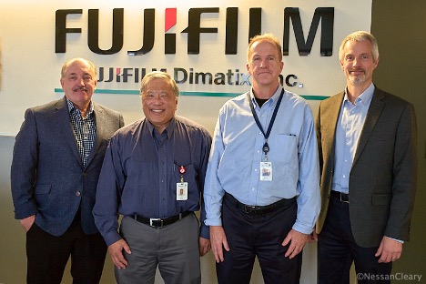
From left: Dave Pulizzi, vp of operations; Darren Imai, VP of MEMs R&D; Terry O’Keefe, senior product manager; and Bailey Smith, EVP business development.
Terry O’Keefe, senior product manager for the Samba printheads, says that the MEMs fabrication is an intrinsic part of the Samba’s feature set, noting: “As we get smaller and smaller drops and all the problems from turbulence, we want to have all those nozzles as close together as we can. And the faster you run then all that becomes more important. And being able to put all these features into a small space, that’s one of the characteristics of MEMs.”
O’Keefe says that the material set has to be chemically compatible with the bulk of fluids that customers use, noting: “We do everything in house. All the way through from design to testing. We have people who are experts at designing jets. We can test it through a process and get some information and that’s all done in-house.”
Smith elaborates: “We have put a lot of effort into our materials testing. We want to be able to predict what a jet will do. There is a lot of energy in producing the droplets but that creates some feedback and cross talk between the nozzles. We have developed a lot of production tools that are better than anything else on the market.”
In conclusion, the Dimatix fab in Santa Clara is extremely impressive. It’s almost entirely dedicated to building the Samba printheads. The whole facility runs 24/7 and employs around 300 people. The ceilings are lined with pipes and cabling and there are dedicated rooms for each separate process, including a dedicated clean area. The recent updates have ensured that Dimatix has enough capacity to address its needs up to 2027. Dave Pulizzi, vice president of operations for the Santa Clara plant, says: “And we have the plans in place to go beyond that if and when it’s necessary.”
There’s a follow-up to this story still to come where I will look in more detail at the Samba head and how it has benefited from Fujifilm’s decision to pursue the MEMs approach and how this translates into the current crop of single pass inkjet presses. In the meantime you can find more details from fujifilm.com.